PTH / PANEL- AND PATTERN PLATING
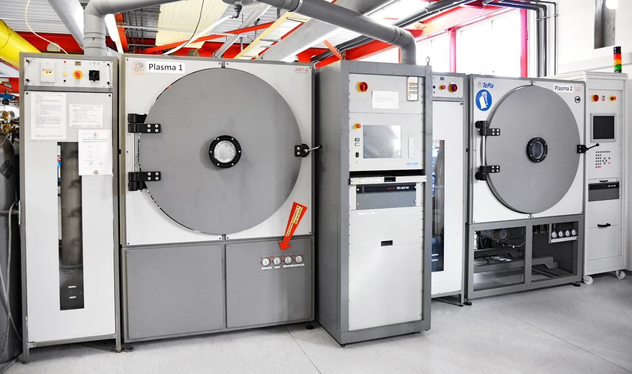
Plasma
The pre-treatment for vias in special materials such as polyimide, Teflon, adhesives and hybrid structures takes place in plasma ovens. If necessary, surface cleaning can be carried out in oxygen plasma.
| plate thickness | 0.050 – 6.0 mm |
 |
|
| format | max. 610 x 530 mm min. depending on panel thickness |
 |
|
| capacity | 1400 m² / day |


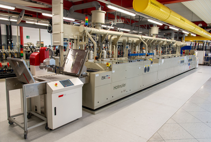
Desmear / etch back
| format | max. 650 x 1500 mm min.100 x 200 mm |
 |
|
| plate thickness | 0.050 – 8.5 mm |
 |
|
| capacity | 850 m² / day |
 |
|
| Reel to Reel | max. bandwidth 650 mm |

Via vertical
| format | max. 650 x 1500 mm min.100 x 200 mm |
 |
|
| plate thickness | 0.050 – 15.0 mm |
 |
|
| capacity | 200 – 250 m² / day |
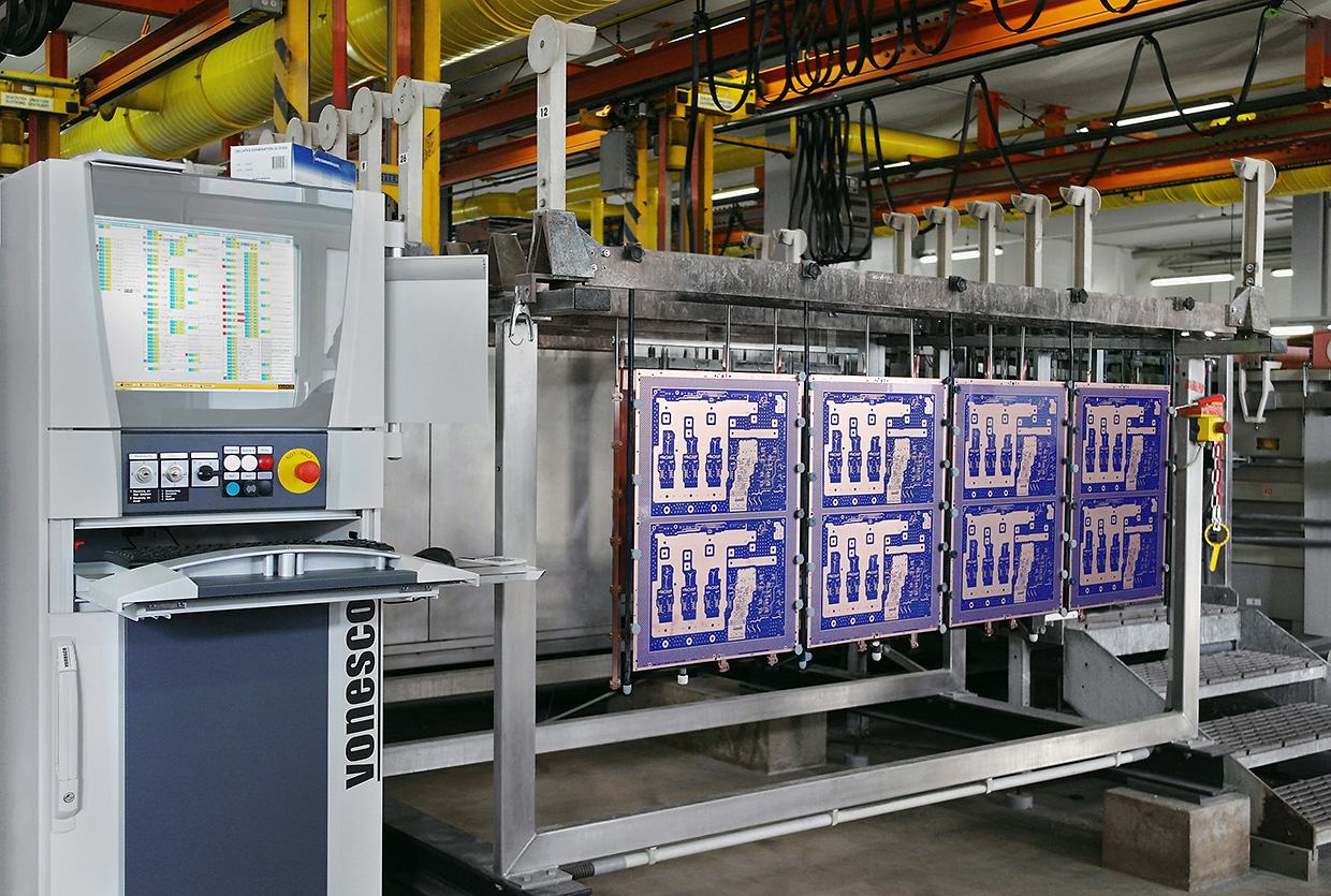
Vertical Plating DPL-3
| format | max. 650 x 1400 mm min. 100 x 200 mm |
 |
|
| plate thickness | 0.012 – 15.0 mm |
 |
|
| capacity | 200 – 250 m² / day |


DK horizontal / plating horizontal
| format | max. 650 x 2000 mm min. 350 x 220 mm |
 |
|
| plate thickness | max. 3.0 mm min. 0.1 mm |
 |
|
| Aspect ratio drilling |
1:12 |
 |
|
| Aspect Ratio Vais |
1:1 |
 |
|
| capacity |
150 – 200 m² / day |
 |
|
| Reel to Reel |
max. bandwidth 650 mm |
conductive pattern construction
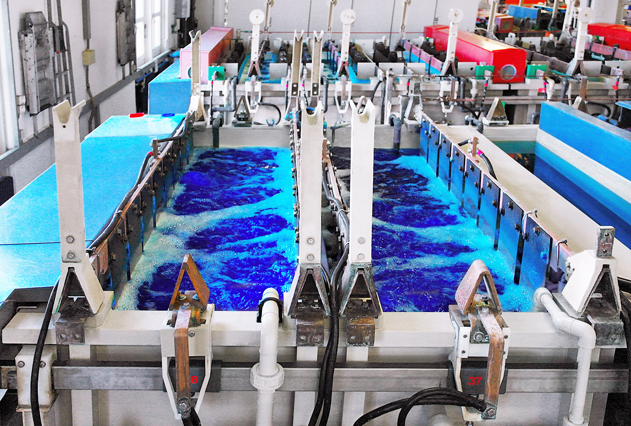
Based on one of the direct metallization methods or galvanically prepared copper bores, we selectively build up the structured circuit patterns (pattern plating). The flexible system control makes it possible to apply different layer thicknesses or etching resists (pure tin or tin 60 / lead 40). The copper baths are operated with a pulse plating electrolyte.
| format | max. 700 x 2000 mm min. 200 x 200 mm |
 |
|
| plate Thickness | 0.05 – 15 mm |
 |
|
| covers |
all known photoresists (Printing colors after testing) |
 |
|
| Aspect ratio drilling |
1:10 (higher after pre-test) |
 |
|
| Blind microvias | 1:1 |
 |
|
| capacity |
200 m² / day |


Microfill 2
This process allows blind microvias to be filled at the same time as through-holes to be reinforced. With the use of photoresists, a selective conductive pattern can be built up.
| format | max. 650 x 2000 mm min. 200 x 100 mm |
 |
|
| plate Thickness | 0.050 – 15.0 mm |
 |
|
| Aspect ratio drilling |
1:10 |
 |
|
| Blind Microvia |
Ø 70 – 120 μm |
 |
|
| Aspect Ratio | bis 1:1 |
 |
|
| layer thickness surface | depending on Ø and degree of filling |
 |
|
| capacity | on request |
THF – Through hole filling
THF – Electrolytically fill through-holes with copper
With this process, which consists of 2 separate process stages, through-holes can be 100% filled with copper, whereby the copper layer thickness on the surface increases comparatively minimally
Filling the continuous bores with copper improves their thermal and electrical conductivity considerably.
PCBs with copper filled through holes have excellent reliability and can easily withstand the currents used in high power, high frequency, microwave and LED PCBs.
| format | max. 610 x 460 mm min. 200 x 200 mm |
 |
|
| plate Thickness | 0.025 – 0.8 mm |

